THB6128 Development Specification Proposal
1.Application: PWM current control stepping motor driver
2.Package: MFP30KR
3.Features
z1 channel PWM current control stepping motor driver
zBiCDMOS process IC
zOutput on-resistance( High side 0.3 Ω, Low side 0.25 Ω, Total 0.55 Ω; Ta = 25°C, Io = 2.0 A)
z2, 1-2, W1-2, 2W1-2, 4W1-2, 8W1-2, 16W1-2, 32W1-2 phase excitation are selectable
zAdvance the excitation step with the only step signal input
zAvailable forward reverse control
zIomax=2.2A
zOver current protection circuit
zThermal shutdown circuit
zInput pull down resistance
zWith reset pin and enable pin
4.Absolute Maximum Ratings at Ta = 25°C
Parameter |
Symbol |
Ratings |
Unit |
Supply voltage |
VMmax |
36 |
V |
Output current |
Iomax |
2.2 |
A |
Logic input voltage |
VINmax |
6 |
V |
VREF input voltage |
VREFmax |
3 |
V |
MO input voltage |
VMOmax |
6 |
V |
DOWN input voltage |
VDOmax |
6 |
V |
Operating temperature |
Topg |
-20 to +85 |
°C |
Storage temperature |
Tstg |
-55 to +150 |
°C |
5. Recommended Operating Range at Ta=25°C |
|
|
|
|
|
|
Parameter |
Symbol |
Ratings |
Unit |
Supply voltage range |
VM |
9 to 32 |
V |
Logic input voltage range |
VIN |
0 to 5 |
V |
VREF input voltage range |
VREF |
0 to 3 |
V |
1
6. Electrical Characteristics at Ta =25°C, VM=24V, VREF=1.5V
Parameter |
Symbol |
Conditions |
min |
typ |
max |
Unit |
Standby mode current drain |
IMstn |
ST=”L” |
|
70 |
|
μA |
current drain |
IM |
ST=”H”,OE=”H”, no load |
|
4 |
|
mA |
Thermal shutdown |
TSD |
Design guarantee |
|
180 |
|
°C |
temperature |
|
|
|
|
|
|
Thermal hysteresis width |
TSD |
Design guarantee |
|
40 |
|
°C |
Logic pin input current |
IinL1 |
VIN=0.8V |
|
8 |
|
μA |
|
IinH1 |
VIN=5V |
|
50 |
|
μA |
Logic input high-level |
Vinh |
|
2.0 |
|
|
V |
voltage |
|
|
|
|
|
|
Logic input low-level |
Vinl |
|
|
|
0.8 |
V |
voltage |
|
|
|
|
|
|
FDT pin high-level voltage |
Vfdth |
|
3.5 |
|
|
V |
FDT pin middle-level |
Vfdtm |
|
1.1 |
|
3.1 |
V |
voltage |
|
|
|
|
|
|
FDT pin low-level voltage |
Vfdtl |
|
|
|
0.8 |
V |
Chopping frequency |
Fch |
Cosc1=100pF |
|
100 |
|
KHz |
OSC1 pin charge/discharge |
Iosc1 |
|
|
10 |
|
μA |
current |
|
|
|
|
|
|
Chopping oscillator circuit |
Vtup1 |
|
|
1 |
|
V |
threshold voltage |
Vtdown1 |
|
|
0.5 |
|
V |
VREF pin input voltage |
Iref |
VREF=1.5V |
-0.5 |
|
|
μA |
DOWN output residual |
VolDO |
Idown=1mA |
|
|
400 |
mV |
voltage |
|
|
|
|
|
|
MO pin residual voltage |
VolMO |
Imo=1mA |
|
|
400 |
mV |
Hold current switching |
Falert |
Cosc2=1500pF |
|
1.6 |
|
Hz |
frequency |
|
|
|
|
|
|
OSC2 pin charge/discharge |
Iosc2 |
|
|
10 |
|
μA |
current |
|
|
|
|
|
|
Hold current switching |
Vtup2 |
|
|
1 |
|
V |
frequency threshold voltage |
Vtdown2 |
|
|
0.5 |
|
V |
REG1 output voltage |
Vreg1 |
|
|
5 |
|
V |
REG2 output voltage |
Vreg2 |
|
|
19 |
|
V |
Blanking time |
Tbl |
|
|
1 |
|
uS |
Output block |
|
|
|
|
|
|
Output on-resistance |
Ronu |
Io=2.0A, high-side ON resistance |
|
0.3 |
|
Ω |
|
Rond |
Io=2.0A, low-side ON resistance |
|
0.25 |
|
Ω |
Output leakage current |
Ioleak |
VM=36V |
|
|
50 |
μA |
Diode forward voltage |
VD |
ID=-2.0A |
|
1 |
|
V |
Current setting reference |
VRF |
VREF=1.5V, Current ratio 100% |
|
300 |
|
mV |
voltage |
|
|
|
|
|
|
Output short-circuit protection |
block |
|
|
|
|
|
Timer latch time |
Tscp |
|
|
256 |
|
μs |
2
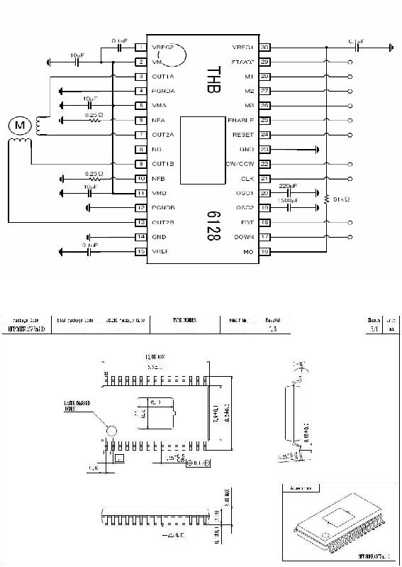
7. PIN ARRANGEMENT (Proposal)
|
|
|
|
|
|
1 |
VREG2 |
|
VREG1 |
30 |
2 |
|
|
ST/VCC |
29 |
VM |
3 |
OUT1A |
M1 |
28 |
4 |
PGNDA |
M2 |
27 |
5 |
VMA |
M3 |
26 |
6 |
NFA |
ENABLE |
25 |
7 |
OUT2A |
RESET |
24 |
8 |
NC |
GND |
23 |
9 |
OUT1B |
CW/CCW |
22 |
10 |
NFB |
CLK |
21 |
11 |
VMB |
OSC1 |
20 |
12 |
PGNDB |
OSC2 |
19 |
13 |
OUT2B |
FDT |
18 |
14 |
GND |
DOWN |
17 |
15 |
VREF |
MO |
16 |
3
8. Pin Functions
Pin No. |
Pin symbol |
Pin Functions |
17 |
DOWN |
Holding current output |
14,23 |
SGND |
Signal GND |
20 |
OSC1 |
Chopping frequency setting capacitor connection |
18 |
FDT |
Decay mode select voltage input |
15 |
VREF |
Constant-current control reference voltage input |
11 |
VMB |
B phase motor supply connection |
28 |
M1 |
Excitation-mode switching pin |
27 |
M2 |
Excitation-mode switching pin |
26 |
M3 |
Excitation-mode switching pin |
13 |
OUT2B |
B phase OUTB output |
10 |
NFB |
B phase current sense resistance connection |
9 |
OUT1B |
B phase OUTA output |
12 |
PGNDB |
B phase power GND |
7 |
OUT2A |
A phase OUTB output |
6 |
NFA |
A phase current sense resistance connection |
3 |
OUT1A |
A phase OUTA output |
4 |
PGNDA |
A phase power GND |
25 |
ENABLE |
Output enable signal input |
24 |
RESET |
RESET signal input |
5 |
VMA |
A phase motor supply connection |
21 |
CLK |
Clock pulse signal input |
22 |
CW/CCW |
Forward/Reverse signal input |
19 |
OSC2 |
Holding current detection time setting capacitor connection |
16 |
MO |
Position detecting monitor |
30 |
VREG1 |
Internal regulator capacitor connection |
1 |
VREG2 |
Internal regulator capacitor connection |
2 |
VM |
Motor power connection |
29 |
ST/VCC |
Chip enable input |
4
9. Description of functions
9-1) Stand-by function
When ST/VCC pin is at low levels, the IC enters stand-by mode, all logic is reset and output is turned OFF. When ST/VCC pin is at high levels, the stand-by mode is released.
9-2) Step pin function
CLK pin step signal input allows advancing excitation step.
Input |
|
|
|
Operation |
ST/VCC |
|
CLK |
|
L |
|
* |
|
Stand-by mode |
H |
|
|
|
|
Excitation step feed |
|
|
|
|
|
|
|
|
|
|
|
|
|
|
|
|
H |
|
|
|
|
Excitation step hold |
|
|
|
|
|
|
|
|
|
|
|
|
|
|
|
|
9-3) Excitation setting method
Set the excitation setting as shown in the following table by setting M1 pin, M2 pin and M3 pin.
|
Input |
|
Mode |
Initial position |
M3 |
M2 |
M1 |
(Excitation) |
A phase current |
B phase current |
L |
L |
L |
2 phase |
100% |
-100% |
L |
L |
H |
1-2 phase |
100% |
0% |
L |
H |
L |
W1-2 phase |
100% |
0% |
L |
H |
H |
2W1-2 phase |
100% |
0% |
H |
L |
L |
4W1-2 phase |
100% |
0% |
H |
L |
H |
8W1-2 phase |
100% |
0% |
H |
H |
L |
16W1-2 phase |
100% |
0% |
H |
H |
H |
32W1-2 phase |
100% |
0% |
The initial position is also the default state at start-up and excitation position at counter-reset in each excitation mode.
9-4) Output current setting
Output current is set as shown below by the VREF pin (applied voltage) and a resistance value between NFA (B) pin and GND.
Iout = (VREF / 5)/ NFA (B) resistance
※* The setting value above is a 100% output current in each excitation mode.
(Example) When VREF=1.5V and NFA (B) resistance is 0.3 Ω, the setting current is shown below. Iout = (1.5 V / 5) / 0.3 Ω = 1.0 A
5
9-5) Output enable function
When the ENABLE pin is set Low, the output is forced OFF and goes to high impedance. However, the internal logic circuits are operating, so the excitation position proceeds when the CLK is input. Therefore, when ENABLE pin is returned to High, the output level conforms to the excitation position proceeded by the CLK input.
ENABLE
CLK
MO
A phase outpu t
0%
B ph ase output
High impeda nce outpu t
9-6) Reset function
When the RESET pin is set Low, the output goes to initial mode and the excitation position is fixed in the initial position for CLK pin and CW/CCW pin input. MO pin outputs at low levels at the initial position. (Open drain connection)
RESET
CLK
MO
A phase outpu t
0 %
B phase ou tput
Initial position
6
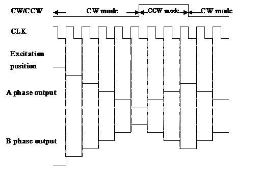
9-7) Forward/reverse switching function
CW/CCW |
Operation |
L |
CW |
H |
CCW |
The internal D/A converter proceeds by a bit on the rising edge of the step signal input to the CLK pin. In addition, CW and CCW mode are switched by CW and CCW pin setting.
In CW mode, the B phase current is delayed by 90°relative to the A phase current. In CCW mode, the B phase current is advanced by 90°relative to the A phase current.
9-8) DECAY mode setting
Current DECAY method is selectable as shown below by applied voltage to the FDT pin.
FDT voltage |
DECAY method |
3.5V to |
SLOW DECAY |
1.1V to 3.1V |
|
or OPEN |
MIXED DECAY |
to 0.8V |
FAST DECAY |
9-9) DOWN, MO output pin
Output pin is an open drain connection. Each pin is turned ON at predetermined state and outputs at low levels.
Pin state |
DOWN |
MO |
Low |
Holding |
Initial position |
current state |
|
|
Non initial |
OFF |
Normal state |
position |
7
9-10) Chopping frequency setting function
Chopping frequency is set as shown below by a capacitor between OSC1 pin and GND. Fcp = 1 / (Cosc1 / 10×10-6) (Hz)
(Example) When Cosc1=100pF, the chopping frequency is shown below. Fcp = 1 / (100×10-12 / 10×10-6) = 100 (kHz)
9-11) Output current vector locus (1 step normalized 90°)
|
100.0 |
|
|
|
|
|
|
θ0 |
θ8 |
θ16 |
|
|
θ64' |
|
θ24 |
|
(2PHASE) |
|
|
|
|
|
|
|
|
|
θ32 |
|
|
|
|
|
|
|
θ40 |
|
|
|
|
|
|
θ48 |
|
|
|
|
|
|
θ56 |
|
(%) |
66.7 |
|
|
|
θ64 |
|
|
|
|
|
|
ratio |
|
|
|
|
θ72 |
|
|
|
|
|
|
A current |
|
|
|
|
|
θ80 |
|
|
|
|
|
θ88 |
|
|
|
|
|
|
hase |
|
|
|
|
|
θ96 |
33.3 |
|
|
|
|
|
P |
|
|
|
|
|
|
|
|
|
|
θ104 |
|
|
|
|
|
|
|
|
|
|
|
|
θ112 |
|
|
|
|
|
|
θ120 |
|
0.0 |
|
|
|
|
θ128 |
|
|
|
|
|
|
|
0.0 |
|
|
33.3 |
66.7 |
100.0 |
P hase B current ratio (%)
8
Current setting ratio in each excitation mode
|
32W1-2 phase(% |
16W1-2 phase(%) |
8W1-2 phase(%) |
4W1-2 phase(%) |
2W1-2 phase(%) |
W1-2 phase(%) |
1-2 phase(%) |
2 phase(%) |
|
2W1-2 phase(%16W1-2 phase(%) |
8W1-2 phase(%) |
4W1-2 phase(%) |
2W1-2 phase(%) |
W1-2 phase(%) |
1-2 phase(% |
2 phase(%) |
STEP |
Ach |
Bch |
Ach |
Bch |
Ach |
Bch |
Ach |
Bch |
Ach |
Bch |
Ach |
Bch |
Ach |
Bch |
Ach |
Bch |
STEP |
Ach |
Bch |
Ach |
Bch |
Ach |
Bch |
Ach |
Bch |
Ach |
Bch |
Ach |
Bch |
Ach |
Bch |
Ach |
Bch |
θ0 |
100 |
0 |
100 |
0 |
100 |
0 |
100 |
0 |
100 |
0 |
100 |
0 |
100 |
0 |
|
|
θ65 |
70 |
72 |
|
|
|
|
|
|
|
|
|
|
|
|
|
|
θ1 |
100 |
1 |
|
|
|
|
|
|
|
|
|
|
|
|
|
|
θ66 |
69 |
72 |
69 |
72 |
|
|
|
|
|
|
|
|
|
|
|
|
θ2 |
100 |
2 |
100 |
2 |
|
|
|
|
|
|
|
|
|
|
|
|
θ67 |
68 |
73 |
|
|
|
|
|
|
|
|
|
|
|
|
|
|
θ3 |
100 |
4 |
|
|
|
|
|
|
|
|
|
|
|
|
|
|
θ68 |
67 |
74 |
67 |
74 |
67 |
74 |
|
|
|
|
|
|
|
|
|
|
θ4 |
100 |
5 |
100 |
5 |
100 |
5 |
|
|
|
|
|
|
|
|
|
|
θ69 |
66 |
75 |
|
|
|
|
|
|
|
|
|
|
|
|
|
|
θ5 |
100 |
6 |
|
|
|
|
|
|
|
|
|
|
|
|
|
|
θ70 |
65 |
76 |
65 |
76 |
|
|
|
|
|
|
|
|
|
|
|
|
θ6 |
100 |
7 |
100 |
7 |
|
|
|
|
|
|
|
|
|
|
|
|
θ71 |
64 |
77 |
|
|
|
|
|
|
|
|
|
|
|
|
|
|
θ7 |
100 |
9 |
|
|
|
|
|
|
|
|
|
|
|
|
|
|
θ72 |
63 |
77 |
63 |
77 |
63 |
77 |
63 |
77 |
|
|
|
|
|
|
|
|
θ8 |
100 |
10 |
100 |
10 |
100 |
10 |
100 |
10 |
|
|
|
|
|
|
|
|
θ73 |
62 |
78 |
|
|
|
|
|
|
|
|
|
|
|
|
|
|
θ9 |
99 |
11 |
|
|
|
|
|
|
|
|
|
|
|
|
|
|
θ74 |
62 |
79 |
62 |
79 |
|
|
|
|
|
|
|
|
|
|
|
|
θ10 |
99 |
12 |
99 |
12 |
|
|
|
|
|
|
|
|
|
|
|
|
θ75 |
61 |
80 |
|
|
|
|
|
|
|
|
|
|
|
|
|
|
θ11 |
99 |
13 |
|
|
|
|
|
|
|
|
|
|
|
|
|
|
θ76 |
60 |
80 |
60 |
80 |
60 |
80 |
|
|
|
|
|
|
|
|
|
|
θ12 |
99 |
15 |
99 |
15 |
99 |
15 |
|
|
|
|
|
|
|
|
|
|
θ77 |
59 |
81 |
|
|
|
|
|
|
|
|
|
|
|
|
|
|
θ13 |
99 |
16 |
|
|
|
|
|
|
|
|
|
|
|
|
|
|
θ78 |
58 |
82 |
58 |
82 |
|
|
|
|
|
|
|
|
|
|
|
|
θ14 |
99 |
17 |
99 |
17 |
|
|
|
|
|
|
|
|
|
|
|
|
θ79 |
57 |
82 |
|
|
|
|
|
|
|
|
|
|
|
|
|
|
θ15 |
98 |
18 |
|
|
|
|
|
|
|
|
|
|
|
|
|
|
θ80 |
56 |
83 |
56 |
83 |
56 |
83 |
56 |
83 |
56 |
83 |
|
|
|
|
|
|
θ16 |
98 |
20 |
98 |
20 |
98 |
20 |
98 |
20 |
98 |
20 |
|
|
|
|
|
|
θ81 |
55 |
84 |
|
|
|
|
|
|
|
|
|
|
|
|
|
|
θ17 |
98 |
21 |
|
|
|
|
|
|
|
|
|
|
|
|
|
|
θ82 |
53 |
84 |
53 |
84 |
|
|
|
|
|
|
|
|
|
|
|
|
θ18 |
98 |
22 |
98 |
22 |
|
|
|
|
|
|
|
|
|
|
|
|
θ83 |
52 |
85 |
|
|
|
|
|
|
|
|
|
|
|
|
|
|
θ19 |
97 |
23 |
|
|
|
|
|
|
|
|
|
|
|
|
|
|
θ84 |
51 |
86 |
51 |
86 |
51 |
86 |
|
|
|
|
|
|
|
|
|
|
θ20 |
97 |
24 |
97 |
24 |
97 |
24 |
|
|
|
|
|
|
|
|
|
|
θ85 |
50 |
86 |
|
|
|
|
|
|
|
|
|
|
|
|
|
|
θ21 |
97 |
25 |
|
|
|
|
|
|
|
|
|
|
|
|
|
|
θ86 |
49 |
87 |
49 |
87 |
|
|
|
|
|
|
|
|
|
|
|
|
θ22 |
96 |
27 |
96 |
27 |
|
|
|
|
|
|
|
|
|
|
|
|
θ87 |
48 |
88 |
|
|
|
|
|
|
|
|
|
|
|
|
|
|
θ23 |
96 |
28 |
|
|
|
|
|
|
|
|
|
|
|
|
|
|
θ88 |
47 |
88 |
47 |
88 |
47 |
88 |
47 |
88 |
|
|
|
|
|
|
|
|
θ24 |
96 |
29 |
96 |
29 |
96 |
29 |
96 |
29 |
|
|
|
|
|
|
|
|
θ89 |
46 |
89 |
|
|
|
|
|
|
|
|
|
|
|
|
|
|
θ25 |
95 |
30 |
|
|
|
|
|
|
|
|
|
|
|
|
|
|
θ90 |
45 |
89 |
45 |
89 |
|
|
|
|
|
|
|
|
|
|
|
|
θ26 |
95 |
31 |
95 |
31 |
|
|
|
|
|
|
|
|
|
|
|
|
θ91 |
44 |
90 |
|
|
|
|
|
|
|
|
|
|
|
|
|
|
θ27 |
95 |
33 |
|
|
|
|
|
|
|
|
|
|
|
|
|
|
θ92 |
43 |
90 |
43 |
90 |
43 |
90 |
|
|
|
|
|
|
|
|
|
|
θ28 |
94 |
34 |
94 |
34 |
94 |
34 |
|
|
|
|
|
|
|
|
|
|
θ93 |
42 |
91 |
|
|
|
|
|
|
|
|
|
|
|
|
|
|
θ29 |
94 |
35 |
|
|
|
|
|
|
|
|
|
|
|
|
|
|
θ94 |
41 |
91 |
41 |
91 |
|
|
|
|
|
|
|
|
|
|
|
|
θ30 |
93 |
36 |
93 |
36 |
|
|
|
|
|
|
|
|
|
|
|
|
θ95 |
39 |
92 |
|
|
|
|
|
|
|
|
|
|
|
|
|
|
θ31 |
93 |
37 |
|
|
|
|
|
|
|
|
|
|
|
|
|
|
θ96 |
38 |
92 |
38 |
92 |
38 |
92 |
38 |
92 |
38 |
92 |
38 |
92 |
|
|
|
|
θ32 |
92 |
38 |
92 |
38 |
92 |
38 |
92 |
38 |
92 |
38 |
92 |
38 |
|
|
|
|
θ97 |
37 |
93 |
|
|
|
|
|
|
|
|
|
|
|
|
|
|
θ33 |
92 |
39 |
|
|
|
|
|
|
|
|
|
|
|
|
|
|
θ98 |
36 |
93 |
36 |
93 |
|
|
|
|
|
|
|
|
|
|
|
|
θ34 |
91 |
41 |
91 |
41 |
|
|
|
|
|
|
|
|
|
|
|
|
θ99 |
35 |
94 |
|
|
|
|
|
|
|
|
|
|
|
|
|
|
θ35 |
91 |
42 |
|
|
|
|
|
|
|
|
|
|
|
|
|
|
θ100 |
34 |
94 |
34 |
94 |
34 |
94 |
|
|
|
|
|
|
|
|
|
|
θ36 |
90 |
43 |
90 |
43 |
90 |
43 |
|
|
|
|
|
|
|
|
|
|
θ101 |
33 |
95 |
|
|
|
|
|
|
|
|
|
|
|
|
|
|
θ37 |
90 |
44 |
|
|
|
|
|
|
|
|
|
|
|
|
|
|
θ102 |
31 |
95 |
31 |
95 |
|
|
|
|
|
|
|
|
|
|
|
|
θ38 |
89 |
45 |
89 |
45 |
|
|
|
|
|
|
|
|
|
|
|
|
θ103 |
30 |
95 |
|
|
|
|
|
|
|
|
|
|
|
|
|
|
θ39 |
89 |
46 |
|
|
|
|
|
|
|
|
|
|
|
|
|
|
θ104 |
29 |
96 |
29 |
96 |
29 |
96 |
29 |
96 |
|
|
|
|
|
|
|
|
θ40 |
88 |
47 |
88 |
47 |
88 |
47 |
88 |
47 |
|
|
|
|
|
|
|
|
θ105 |
28 |
96 |
|
|
|
|
|
|
|
|
|
|
|
|
|
|
θ41 |
88 |
48 |
|
|
|
|
|
|
|
|
|
|
|
|
|
|
θ106 |
27 |
96 |
27 |
96 |
|
|
|
|
|
|
|
|
|
|
|
|
θ42 |
87 |
49 |
87 |
49 |
|
|
|
|
|
|
|
|
|
|
|
|
θ107 |
25 |
97 |
|
|
|
|
|
|
|
|
|
|
|
|
|
|
θ43 |
86 |
50 |
|
|
|
|
|
|
|
|
|
|
|
|
|
|
θ108 |
24 |
97 |
24 |
97 |
24 |
97 |
|
|
|
|
|
|
|
|
|
|
θ44 |
86 |
51 |
86 |
51 |
86 |
51 |
|
|
|
|
|
|
|
|
|
|
θ109 |
23 |
97 |
|
|
|
|
|
|
|
|
|
|
|
|
|
|
θ45 |
85 |
52 |
|
|
|
|
|
|
|
|
|
|
|
|
|
|
θ110 |
22 |
98 |
22 |
98 |
|
|
|
|
|
|
|
|
|
|
|
|
θ46 |
84 |
53 |
84 |
53 |
|
|
|
|
|
|
|
|
|
|
|
|
θ111 |
21 |
98 |
|
|
|
|
|
|
|
|
|
|
|
|
|
|
θ47 |
84 |
55 |
|
|
|
|
|
|
|
|
|
|
|
|
|
|
θ112 |
20 |
98 |
20 |
98 |
20 |
98 |
20 |
98 |
20 |
98 |
|
|
|
|
|
|
θ48 |
83 |
56 |
83 |
56 |
83 |
56 |
83 |
56 |
83 |
56 |
|
|
|
|
|
|
θ113 |
18 |
98 |
|
|
|
|
|
|
|
|
|
|
|
|
|
|
θ49 |
82 |
57 |
|
|
|
|
|
|
|
|
|
|
|
|
|
|
θ114 |
17 |
99 |
17 |
99 |
|
|
|
|
|
|
|
|
|
|
|
|
θ50 |
82 |
58 |
82 |
58 |
|
|
|
|
|
|
|
|
|
|
|
|
θ115 |
16 |
99 |
|
|
|
|
|
|
|
|
|
|
|
|
|
|
θ51 |
81 |
59 |
|
|
|
|
|
|
|
|
|
|
|
|
|
|
θ116 |
15 |
99 |
15 |
99 |
15 |
99 |
|
|
|
|
|
|
|
|
|
|
θ52 |
80 |
60 |
80 |
60 |
80 |
60 |
|
|
|
|
|
|
|
|
|
|
θ117 |
13 |
99 |
|
|
|
|
|
|
|
|
|
|
|
|
|
|
θ53 |
80 |
61 |
|
|
|
|
|
|
|
|
|
|
|
|
|
|
θ118 |
12 |
99 |
12 |
99 |
|
|
|
|
|
|
|
|
|
|
|
|
θ54 |
79 |
62 |
79 |
62 |
|
|
|
|
|
|
|
|
|
|
|
|
θ119 |
11 |
99 |
|
|
|
|
|
|
|
|
|
|
|
|
|
|
θ55 |
78 |
62 |
|
|
|
|
|
|
|
|
|
|
|
|
|
|
θ120 |
10 |
100 |
10 |
100 |
10 |
100 |
10 |
100 |
|
|
|
|
|
|
|
|
θ56 |
77 |
63 |
77 |
63 |
77 |
63 |
77 |
63 |
|
|
|
|
|
|
|
|
θ121 |
9 |
100 |
|
|
|
|
|
|
|
|
|
|
|
|
|
|
θ57 |
77 |
64 |
|
|
|
|
|
|
|
|
|
|
|
|
|
|
θ122 |
7 |
100 |
7 |
100 |
|
|
|
|
|
|
|
|
|
|
|
|
θ58 |
76 |
65 |
76 |
65 |
|
|
|
|
|
|
|
|
|
|
|
|
θ123 |
6 |
100 |
|
|
|
|
|
|
|
|
|
|
|
|
|
|
θ59 |
75 |
66 |
|
|
|
|
|
|
|
|
|
|
|
|
|
|
θ124 |
5 |
100 |
5 |
100 |
5 |
100 |
|
|
|
|
|
|
|
|
|
|
θ60 |
74 |
67 |
74 |
67 |
74 |
67 |
|
|
|
|
|
|
|
|
|
|
θ125 |
4 |
100 |
|
|
|
|
|
|
|
|
|
|
|
|
|
|
θ61 |
73 |
68 |
|
|
|
|
|
|
|
|
|
|
|
|
|
|
θ126 |
2 |
100 |
2 |
100 |
|
|
|
|
|
|
|
|
|
|
|
|
θ62 |
72 |
69 |
72 |
69 |
|
|
|
|
|
|
|
|
|
|
|
|
θ127 |
1 |
100 |
|
|
|
|
|
|
|
|
|
|
|
|
|
|
θ63 |
72 |
70 |
|
|
|
|
|
|
|
|
|
|
|
|
|
|
θ128 |
0 |
100 |
0 |
100 |
0 |
100 |
0 |
100 |
0 |
100 |
0 |
100 |
0 |
100 |
|
|
θ64 |
71 |
71 |
71 |
71 |
71 |
71 |
71 |
71 |
71 |
71 |
71 |
71 |
71 |
71 |
100 |
100 |
|
|
|
|
|
|
|
|
|
|
|
|
|
|
|
|
|
9
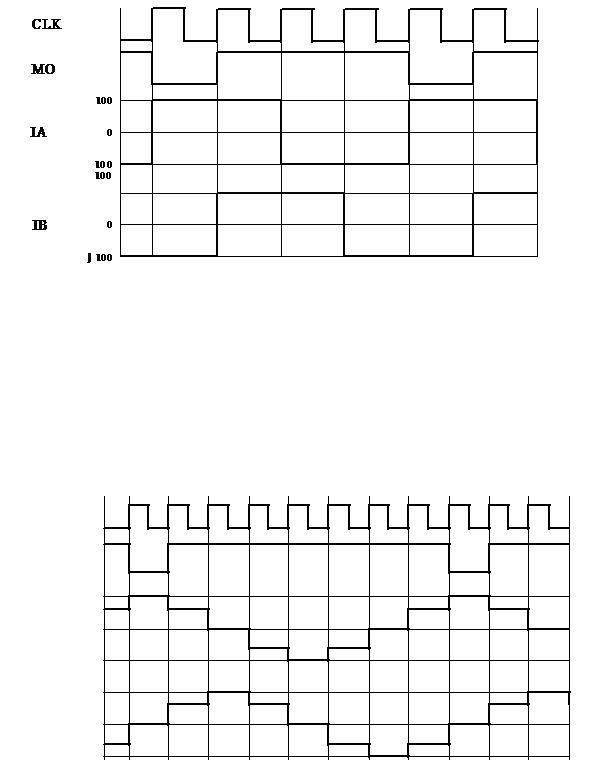
9-12) Current wave example in each excitation mode (2 phase, 1-2 phase, W1-2 phase, 4W1-2 phase) 2 phase excitation (CW mode)
1-2 phase excitation (CW mode)
CLK
MO
(%) 1 00
IA 0
-100
(%) 1 00
IB 0
-100
10
W1-2 phase excitation (CW mode)
CLK
MO
(%) 10 0
IA 0
-1 00
(%)
100
IB 0
-10 0
4W1-2 phase excitation (CW mode)
11
9-13) Output short-circuit protection circuit
Build-in output short-circuit protection circuit makes output to enter in stand-by mode. This function prevents the IC from damaging when the output shorts circuit by a voltage short or a ground short, etc. When output short state is detected, short-circuit detection circuit starts the operating and output is once turned OFF. After the timer latch time (typ: 256us), output is turned ON again. Still the output is at short state, the output is turned OFF and fixed in stand-by mode.
When output is fixed in stand-by mode by output short protection circuit, output is released the latch by setting ST/VCC=”L”.
9-14) Open-drain pin for switching holding current The output pin is an open drain connection.
This pin is turned ON when no rising edge of CLK between the input signals while a period determined by a capacitor between OSC2 and GND, and outputs at low levels.
The open-drain output in once turned ON, is turned OFF at the next rising edge of CLK.
Holding current switching time (Tdown) is set as shown below by a capacitor between OSC2 pin and GND. Tdown = Cosc2 × 0.4×109 (s)
(Example) When Cosc2=1500pF, the holding current switching time is shown below. Tdown = 1500 pF × 0.4×109 = 0.6 (s)
12
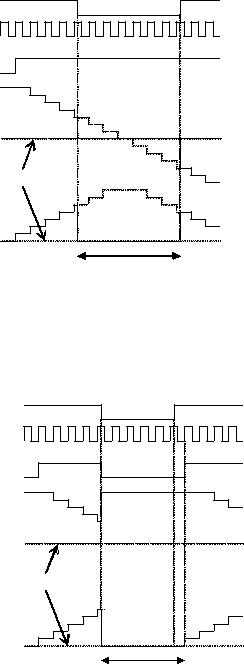
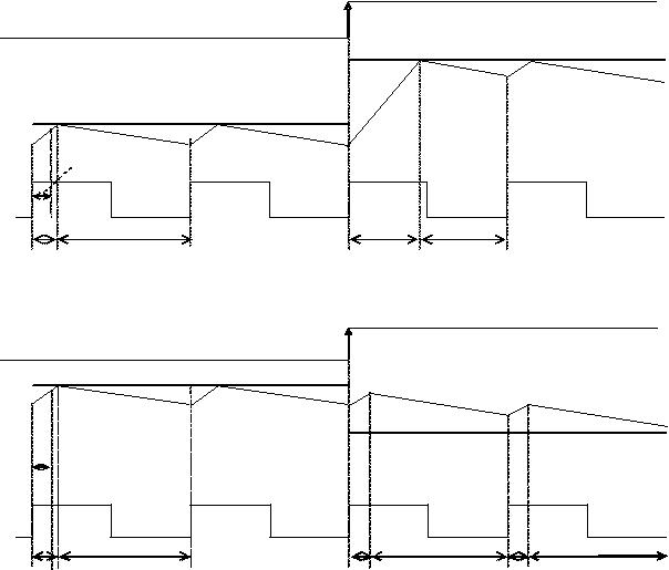
10. Current control operation
10-1) SLOW DECAY current control operation
When FDT pin voltage is a voltage over 3.5 V, the constant-current control is operated in SLOW DECAY mode. (Sine-wave increasing direction)
CLK
S et tin g cu r r e n t
S e t tin g cur re n t
Coil cu rr en t
Bla n k in g T im e
fch op
C u r r e n t m ode C H ARG E SL OW |
CH ARGE |
SL OW |
(Sine-wave decreasing direction)
C L K
S et t i n g cu r r en t
C oil cu r r en t
S e t t in g cu r r e n t
 B l a n k in g T i m e
fch o p
C u r re n t m od e C H A R G E |
S L O W |
B la n k i n g T i m e |
S L O W B l a n k in g T im e |
S L O W |
Each of current modes operates with the follow sequence.
zThe IC enters CHARGE mode at a rising edge of the chopping oscillation.
(A period of CHARGE mode (Blanking Time) is forcibly present in approximately 1 μs, regardless of the current value of the coil current(ICOIL)and set current (IREF)).
zAfter the period of the blanking time, the IC operates in CHARGE mode until ICOIL≥IREF. After that, the mode switches
to the SLOW DECAY mode and the coil current is attenuated until the end of a chopping period.
At the constant-current control in SLOW DECAY mode, following to the setting current from the coil current may take time (or not follow) for the current delay attenuation.
13
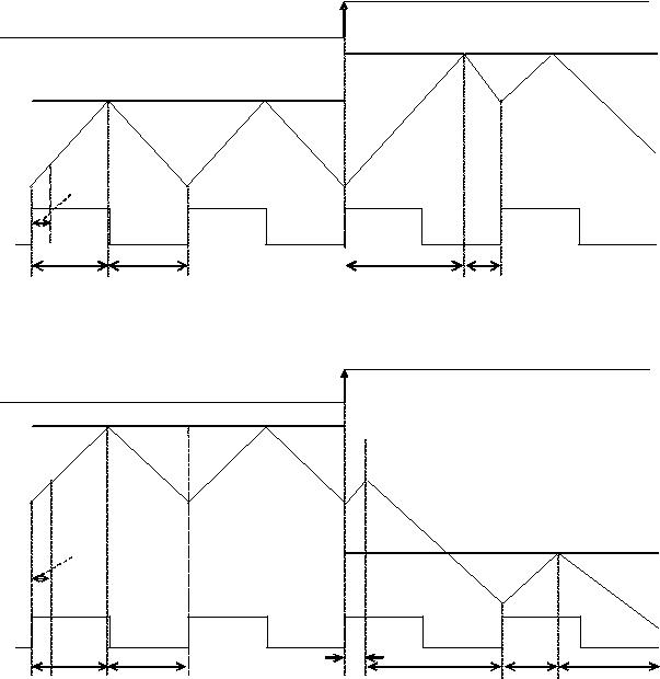
10-2) FAST DECAY current control operation
When FDT pin voltage is a voltage under 0.8V, the constant-current control is operated in FAST DECAY mode. (Sine-wave increasing direction)
CLK
Se ttin g cu r r e n t
S e tt in g cu r r e n t
Coil cu r re n t
Bla n k in g T im e
fch op |
|
|
|
C ur r en t m ode CH ARGE |
FAST |
CH ARGE |
FAST |
(Sine-wave decreasing direction)
C L K
S et t i n g cu r r en t
C oil cu r r e n t
B l a n k in g T i m e |
S e t t i n g cu r r en t |
|
fch o p |
|
|
|
|
|
C u r r e n t m od e C H A R G E |
F A S T |
B la n k i n g T i m e |
F A S T |
C H A R G E |
F A S T |
Each of current modes operates with the follow sequence.
zThe IC enters CHARGE mode at a rising edge of the chopping oscillation.
(A period of CHARGE mode (Blanking Time) is forcibly present in approximately 1 μs, regardless of the current value of the coil current (ICOIL) and set current (IREF)).
zAfter the period of the blanking time, The IC operates in CHARGE mode until ICOIL ≥ IREF. After that, the mode
switches to the FAST DECAY mode and the coil current is attenuated until the end of a chopping period.
At the constant-current control in FAST DECAY mode, following to the setting current from the coil current takes short-time for the current fast attenuation, but, the current ripple value may be higher.
14
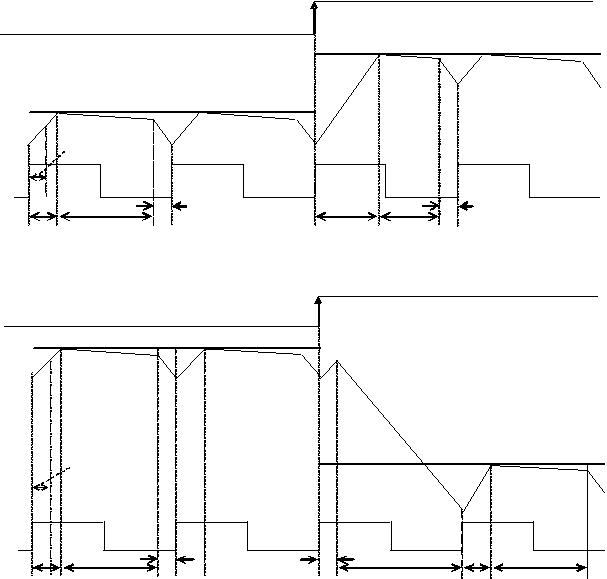
10-3) MIXED DECAY current control operation
When FDT pin voltage is a voltage between 1.1 V to 3.1 V or OPEN, the constant-current control is operated in MIXED DECAY mode. (Sine-wave increasing direction)
STP
S e ttin g cu r r e n t
S e tt in g cu r r e n t
Coil cu rr en t
Bla n k in g T im e
fch op
C u r r en t m ode C H ARG E SL OW |
FAST |
CH ARGE |
SL OW FAST |
(Sine-wave decreasing direction)
C L K
S e t t i n g cu r r e n t
C oi l c u r r e n t
B l a n k in g T im e |
S e t t in g cu r r e n t |
|
fc h op
C u r r e n t m o d e C H A R G E |
S L O W |
FA S T |
B l a n k in g T im e |
F A S T |
C H A R G E |
S L O W |
15
Each of current modes operates with the follow sequence.
zThe IC enters CHARGE mode at a rising edge of the chopping oscillation.
(A period of CHARGE mode (Blanking Time) is forcibly present in approximately 1 μs, regardless of the current value of the coil current (ICOIL) and set current (IREF)).
z In a period of Blanking Time, the coil current (ICOIL) and the setting current (IREF) are compared. If an ICOIL < IREF state exists during the charge period:
The IC operates in CHAGE mode until ICOIL ≥ IREF. After that, it switches to SLOW DECAY mode and then switches to FAST DECAY mode in the last approximately 1 μs of the period.
If no ICOIL < IREF state exists during the charge period:
The IC switches to FAST DECAY mode and the coil current is attenuated with the FAST DECAY operation until the end of a chopping period.
The above operation is repeated.
Normally, in the sine wave increasing direction the IC operates in SLOW (+FAST) DECAY mode, and in the sine wave decreasing direction the IC operates in FAST DECAY mode until the current is attenuated and reaches the set value and the IC operates in SLOW (+FAST) DECAY mode.
11. Block diagram
stage pre Output |
stage pre Output |
stage pre Output |
stage pre Output |
16
12. Wiring diagram
13.Package Dimensions
17